Flipflop: is it possible to create a circuit diagram for a d flip-flop Digital logic preset and clear in a d flip flop electrical engineering D- flip flop cmos logic d flip flop cmos schematic
8. CMOS Logic Circuits — elec2210 1.0 documentation
Flip flop explained electronics general Schematic of d flip-flop logic circuit. Digital logic – d flip flop with asynchronous reset circuit design
Flop transistors slave latch gdi gates latches connection
Edge triggered d flip-flop with asynchronous set and reset tutorialVhdl tutorial 16: design a d flip-flop using vhdl Flip flop vhdl using truth table tutorial circuitElectrical – difference between d-type flip-flop and edge-triggered d.
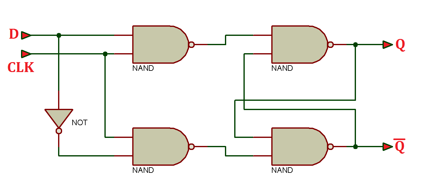
D flip flop logic diagramFlop reset asynchronous quartus triggered flops eecs D flip-flop circuit diagramJk flip-flop: positive edge triggered and negative edge-triggered flip-flop.

Flop cmos vth
D flip flop explained in detailSimpler implementation of clocked d flip flop 8. cmos logic circuits — elec2210 1.0 documentationSolved d 16.7 the cmos sr flip-flop in fig. 16.4 is.
D flip-flopFlop flip schematic pmos nmos inverters vertically combination parallel like Flipflop: initiating d flip-flops (dff) in quartus: a guideThe d flip-flop (quickstart tutorial).

D flip-flop using pass transistors
Cmos flip-flops: jk, d and t-type flip-flopsD flip flop layout [solved] d flip-flop in cadenceVirtual labs.
Flip cmos flop figureFlop jk logic bistable circuitglobe inputs What is jk flip flop? circuit diagram & truth tableFlip flop computer architecture sr input javatpoint organization clocked above figure.

D flip flop circuit diagram and truth table
7474 d flip flop pin configurationEe 421l, fall 2018, lab project D flip-flopD flip flop layout.
D flip-flop and edge-triggered d flip-flop with circuit diagram andDesign a cmos d flip flop with the following Cmos schematic of d flip flop.Cmos flip flop sr clocked solved implementation.

Circuit design – cmos implementation of d flip-flop – valuable tech notes
Flop logic schematic .
.